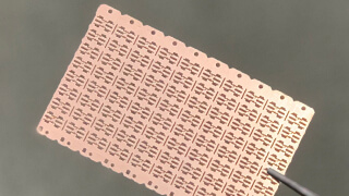
Many printed circuit boards are connected on both sides of the board, and the wiring
patterns are stacked. A technology called “via fill” is used to fill the holes in the substrate with copper
plating. If the plating inhibitor and accelerator are added to the copper sulfate plating additive, the
current will increase, and if there is strong stirring, the plating will slow down due to the function of
the inhibitor, making it difficult for the current to flow in holes, etc. In addition, since the accelerator
works at a weakly stirred place, the plating growth is faster and the holes is filled.


